- 您现在的位置:买卖IC网 > Sheet目录1994 > DS1743P-70+ (Maxim Integrated Products)IC RTC RAM Y2K 5V 70NS 34-PCM
DS1743/DS1743P Y2K-Compliant, Nonvolatile Timekeeping RAMs
7 of 17
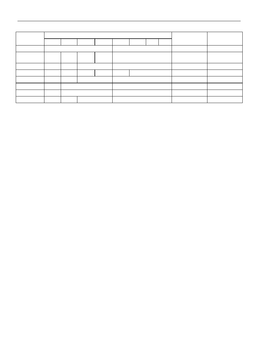
Table 2. Register Map
ADDRESS
DATA
FUNCTION
RANGE
B7
B6
B5
B4
B3
B2
B1
B0
1FFF
10 Year
Year
00–99
1FFE
X
10
Month
01–12
1FFD
X
10 Date
Date
01–31
1FFC
BF
FT
X
Day
01–07
1FFB
X
10 Hour
Hour
00–23
1FFA
X
10 Minutes
Minutes
00–59
1FF9
OSC
10 Seconds
Seconds
00–59
1FF8
W
R
10 Century
Century
Control
00–39
OSC
= STOP BIT
R = READ BIT
FT = FREQUENCY TEST
W = WRITE BIT
X = SEE NOTE BELOW
BF = BATTERY FLAG
Note: All indicated “X” bits must be set to “0” when written to ensure proper clock operation.
RETRIEVING DATA FROM RAM OR CLOCK
The DS1743 is in the read mode whenever OE (output enable) is low, WE (write enable) is high, and CE
(chip enable) is low. The device architecture allows ripple-through access to any of the address locations in
the NV SRAM. Valid data will be available at the DQ pins within tAA after the last address input is stable,
providing that the, CE and OE access times and states are satisfied. If CE, or OE access times and states
are not met, valid data will be available at the latter of chip enable access (tCEA) or at output enable access
time (tCEA). The state of the data input/output pins (DQ) is controlled by CE and OE. If the outputs are
activated before tAA, the data lines are driven to an intermediate state until tAA. If the address inputs are
changed while CE and OE remain valid, output data will remain valid for output data hold time (tOH) but
will then go indeterminate until the next address access.
发布紧急采购,3分钟左右您将得到回复。
相关PDF资料
DS1744-70IND
IC RTC RAM Y2K 5V 70NS 28-EDIP
DS1746-70IND
IC RTC RAM Y2K 5V 70NS 32-EDIP
DS1747W-120IND
IC RTC RAM Y2K 3.3V 120NS 32EDIP
DS17887-3-IND
IC RTC 3V 8K NV RAM 24-EDIP
DS1851E-010+
IC DAC DUAL NV TEMP CNTRL 8TSSOP
DS2187S+
IC RECEIVE LINE INTERFACE 20SOIC
DS21Q58L
IC TXRX E1 QUAD 3.3V 100-LQFP
DS2404B
IC ECONORAM TIMECHIP 5.5V 16SSOP
相关代理商/技术参数
DS1743P-85+
功能描述:实时时钟 Timekeeping NV RAM RoHS:否 制造商:Microchip Technology 功能:Clock, Calendar. Alarm RTC 总线接口:I2C 日期格式:DW:DM:M:Y 时间格式:HH:MM:SS RTC 存储容量:64 B 电源电压-最大:5.5 V 电源电压-最小:1.8 V 最大工作温度:+ 85 C 最小工作温度: 安装风格:Through Hole 封装 / 箱体:PDIP-8 封装:Tube
DS1743P-85IND+
功能描述:实时时钟 Timekeeping NV RAM RoHS:否 制造商:Microchip Technology 功能:Clock, Calendar. Alarm RTC 总线接口:I2C 日期格式:DW:DM:M:Y 时间格式:HH:MM:SS RTC 存储容量:64 B 电源电压-最大:5.5 V 电源电压-最小:1.8 V 最大工作温度:+ 85 C 最小工作温度: 安装风格:Through Hole 封装 / 箱体:PDIP-8 封装:Tube
DS1743P-C01+
制造商:Maxim Integrated Products 功能描述:Y2KC RAM PCAP 8KX8 100NS ROCKWELL - Trays
DS1743W-120
功能描述:实时时钟 RoHS:否 制造商:Microchip Technology 功能:Clock, Calendar. Alarm RTC 总线接口:I2C 日期格式:DW:DM:M:Y 时间格式:HH:MM:SS RTC 存储容量:64 B 电源电压-最大:5.5 V 电源电压-最小:1.8 V 最大工作温度:+ 85 C 最小工作温度: 安装风格:Through Hole 封装 / 箱体:PDIP-8 封装:Tube
DS1743W-120 IND
功能描述:实时时钟 RoHS:否 制造商:Microchip Technology 功能:Clock, Calendar. Alarm RTC 总线接口:I2C 日期格式:DW:DM:M:Y 时间格式:HH:MM:SS RTC 存储容量:64 B 电源电压-最大:5.5 V 电源电压-最小:1.8 V 最大工作温度:+ 85 C 最小工作温度: 安装风格:Through Hole 封装 / 箱体:PDIP-8 封装:Tube
DS1743W-120+
功能描述:实时时钟 Timekeeping NV RAM RoHS:否 制造商:Microchip Technology 功能:Clock, Calendar. Alarm RTC 总线接口:I2C 日期格式:DW:DM:M:Y 时间格式:HH:MM:SS RTC 存储容量:64 B 电源电压-最大:5.5 V 电源电压-最小:1.8 V 最大工作温度:+ 85 C 最小工作温度: 安装风格:Through Hole 封装 / 箱体:PDIP-8 封装:Tube
DS1743W-120IND
功能描述:实时时钟 RoHS:否 制造商:Microchip Technology 功能:Clock, Calendar. Alarm RTC 总线接口:I2C 日期格式:DW:DM:M:Y 时间格式:HH:MM:SS RTC 存储容量:64 B 电源电压-最大:5.5 V 电源电压-最小:1.8 V 最大工作温度:+ 85 C 最小工作温度: 安装风格:Through Hole 封装 / 箱体:PDIP-8 封装:Tube
DS1743W-120IND+
功能描述:实时时钟 Timekeeping NV RAM RoHS:否 制造商:Microchip Technology 功能:Clock, Calendar. Alarm RTC 总线接口:I2C 日期格式:DW:DM:M:Y 时间格式:HH:MM:SS RTC 存储容量:64 B 电源电压-最大:5.5 V 电源电压-最小:1.8 V 最大工作温度:+ 85 C 最小工作温度: 安装风格:Through Hole 封装 / 箱体:PDIP-8 封装:Tube